- 您现在的位置:买卖IC网 > Sheet目录2008 > MAX1279AETC+ (Maxim Integrated Products)IC ADC 12BIT 1.5MSPS 12-TQFN
MAX1277/MAX1279
1.5Msps, Single-Supply, Low-Power, True-
Differential, 12-Bit ADCs with Internal Reference
4
_______________________________________________________________________________________
Note 1: Relative accuracy is the deviation of the analog value at any code from its theoretical value after the gain error and the offset
error have been nulled.
Note 2: No missing codes over temperature.
Note 3: Conversion time is defined as the number of clock cycles (16) multiplied by the clock period.
Note 4: At sample rates below 10ksps, the input full-linear bandwidth is reduced to 5kHz.
Note 5: The listed value of three SCLK cycles is given for full-speed continuous conversions. Acquisition time begins on the 14th ris-
ing edge of SCLK and terminates on the next falling edge of CNVST. The IC idles in acquisition mode between conversions.
Note 6: Undersampling at the maximum signal bandwidth requires the minimum jitter spec for SINAD performance.
Note 7: 1.5Msps operation guaranteed for VL > 2.7V. See the Typical Operating Characteristics section for recommended sampling
speeds for VL < 2.7V.
Note 8: Digital supply current is measured with the VIH level equal to VL, and the VIL level equal to GND.
TIMING CHARACTERISTICS
(VDD = +2.7V to +3.6V, VL = VDD, fSCLK = 24MHz, 50% duty cycle, TA = -40°C to +85°C, unless otherwise noted. Typical values are
at TA = +25°C.)
PARAMETER
SYMBOL
CONDITIONS
MIN
TYP
MAX
UNITS
VL = 2.7V to VDD
18.7
SCLK Pulse-Width High
tCH
VL = 1.8V to VDD, minimum recommended
(Note 7)
22.5
ns
VL = 2.7V to VDD
18.7
SCLK Pulse-Width Low
tCL
VL = 1.8V to VDD, minimum recommended
(Note 7)
22.5
ns
CL = 30pF, VL = 2.7V to VDD
17
SCLK Rise to DOUT Transition
tDOUT
CL = 30pF, VL = 1.8V to VDD
24
ns
DOUT Remains Valid After SCLK
tDHOLD
VL = 1.8V to VDD
4ns
CNVST Fall to SCLK Fall
tSETUP
VL = 1.8V to VDD
10
ns
CNVST Pulse Width
tCSW
VL = 1.8V to VDD
20
ns
Power-Up Time; Full Power-Down
tPWR-UP
2ms
Restart Time; Partial Power-Down
tRCV
16
Cycles
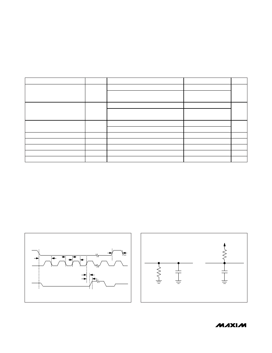
CNVST
SCLK
DOUT
tDHOLD
tDOUT
tSETUP
tCSW
tCL
tCH
Figure 1. Detailed Serial-Interface Timing
GND
6k
Ω
CL
DOUT
CL
GND
VL
a) HIGH-Z TO VOH, VOL TO VOH,
AND VOH TO HIGH-Z
b) HIGH-Z TO VOL, VOH TO VOL,
AND VOL TO HIGH-Z
6k
Ω
Figure 2. Load Circuits for Enable/Disable Times
发布紧急采购,3分钟左右您将得到回复。
相关PDF资料
MAX1285BESA+T
IC ADC 12BIT 300KSPS 8-SOIC
MAX1302BEUG+
IC ADC 16BIT SRL 115KSPS 24TSSOP
MAX1303BEUP+
IC ADC 16BIT MULT RANGE 20TSSOP
MAX1308ECM+T
IC ADC 12BIT 8CH 4MSPS 48LQFP
MAX1320ECM+T
IC ADC 14BIT 8CH 2MSPS 48LQFP
MAX132EWG+T
IC ADC 18BIT SERIAL 24-SOIC
MAX135EPI+
IC ADC 15BIT PARALLEL 28-DIP
MAX1361MEUB+T
IC SYSTEM MON 10BIT 4CH 10-UMAX
相关代理商/技术参数
MAX1279AETC+T
功能描述:模数转换器 - ADC 12-Bit 1.5Msps 3.6V Precision ADC RoHS:否 制造商:Texas Instruments 通道数量:2 结构:Sigma-Delta 转换速率:125 SPs to 8 KSPs 分辨率:24 bit 输入类型:Differential 信噪比:107 dB 接口类型:SPI 工作电源电压:1.7 V to 3.6 V, 2.7 V to 5.25 V 最大工作温度:+ 85 C 安装风格:SMD/SMT 封装 / 箱体:VQFN-32
MAX1279AETC-T
功能描述:模数转换器 - ADC RoHS:否 制造商:Texas Instruments 通道数量:2 结构:Sigma-Delta 转换速率:125 SPs to 8 KSPs 分辨率:24 bit 输入类型:Differential 信噪比:107 dB 接口类型:SPI 工作电源电压:1.7 V to 3.6 V, 2.7 V to 5.25 V 最大工作温度:+ 85 C 安装风格:SMD/SMT 封装 / 箱体:VQFN-32
MAX1279BCTC
功能描述:模数转换器 - ADC RoHS:否 制造商:Texas Instruments 通道数量:2 结构:Sigma-Delta 转换速率:125 SPs to 8 KSPs 分辨率:24 bit 输入类型:Differential 信噪比:107 dB 接口类型:SPI 工作电源电压:1.7 V to 3.6 V, 2.7 V to 5.25 V 最大工作温度:+ 85 C 安装风格:SMD/SMT 封装 / 箱体:VQFN-32
MAX1279BCTC+
功能描述:模数转换器 - ADC Integrated Circuits (ICs) RoHS:否 制造商:Texas Instruments 通道数量:2 结构:Sigma-Delta 转换速率:125 SPs to 8 KSPs 分辨率:24 bit 输入类型:Differential 信噪比:107 dB 接口类型:SPI 工作电源电压:1.7 V to 3.6 V, 2.7 V to 5.25 V 最大工作温度:+ 85 C 安装风格:SMD/SMT 封装 / 箱体:VQFN-32
MAX1279BCTC+T
功能描述:模数转换器 - ADC Integrated Circuits (ICs) RoHS:否 制造商:Texas Instruments 通道数量:2 结构:Sigma-Delta 转换速率:125 SPs to 8 KSPs 分辨率:24 bit 输入类型:Differential 信噪比:107 dB 接口类型:SPI 工作电源电压:1.7 V to 3.6 V, 2.7 V to 5.25 V 最大工作温度:+ 85 C 安装风格:SMD/SMT 封装 / 箱体:VQFN-32
MAX1279BCTC-T
功能描述:模数转换器 - ADC RoHS:否 制造商:Texas Instruments 通道数量:2 结构:Sigma-Delta 转换速率:125 SPs to 8 KSPs 分辨率:24 bit 输入类型:Differential 信噪比:107 dB 接口类型:SPI 工作电源电压:1.7 V to 3.6 V, 2.7 V to 5.25 V 最大工作温度:+ 85 C 安装风格:SMD/SMT 封装 / 箱体:VQFN-32
MAX1279BETC
功能描述:模数转换器 - ADC RoHS:否 制造商:Texas Instruments 通道数量:2 结构:Sigma-Delta 转换速率:125 SPs to 8 KSPs 分辨率:24 bit 输入类型:Differential 信噪比:107 dB 接口类型:SPI 工作电源电压:1.7 V to 3.6 V, 2.7 V to 5.25 V 最大工作温度:+ 85 C 安装风格:SMD/SMT 封装 / 箱体:VQFN-32
MAX1279BETC+
功能描述:模数转换器 - ADC 12-Bit 1.5Msps 3.6V Precision ADC RoHS:否 制造商:Texas Instruments 通道数量:2 结构:Sigma-Delta 转换速率:125 SPs to 8 KSPs 分辨率:24 bit 输入类型:Differential 信噪比:107 dB 接口类型:SPI 工作电源电压:1.7 V to 3.6 V, 2.7 V to 5.25 V 最大工作温度:+ 85 C 安装风格:SMD/SMT 封装 / 箱体:VQFN-32